LLM PCB Routing: Turning a Human's Fixes Into Rules
I handed a 96% auto-routed PCB to a contract engineer. He did not just connect the last 4%, and that difference became 16 rules my agent can reuse.
On this page
- The board
- How far the auto-router got
- A better DRC count can mean a worse board
- Some problems never show up in DRC at all
- What code did far better
- Handing off at 96% auto-routed
- He did not just connect the last 4%
- Layer usage was different too
- How those 11 hole clearance violations went away
- Our own brief was wrong too
- Turning his fixes into the next set of rules
- Testing whether the learned rules get reused
- The human is still better at some of it
- The automation itself was wrong several times
- No evidence the board works yet
- So where do you call a human
I am designing a 21mm circular PCB with an LLM and code.
Placement and auto-routing got me to about 96% of the connections. The last 4% was the problem. A few nets never connected and DRC violations remained. So I paid a PCB engineer KRW 200,000, about USD 145, to finish it.
Comparing the board that came back, the result was not quite what I expected. He did not just connect the remaining 4%. He deleted routing the auto-router considered finished and redrew it, moved nets to different layers, and added vias, reorganizing the whole topology.
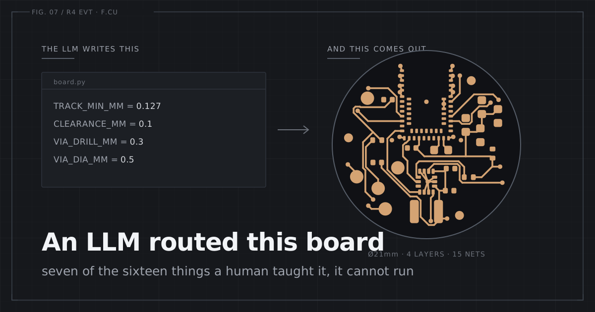
So I compared the two PCBs net by net. I wanted to find what he did differently, then turn that difference into routing rules the agent can reuse on the next board. Sixteen techniques came out of it. Seven of them cannot be executed automatically yet.
This is not a story about an LLM laying out a good board. It is a record of how far the automation got and where human judgement was still required.
Routing decisions ran on Claude Fable 5.
The board
A 21mm circular four-layer PCB. It sits on top of a CR1632 coin cell, so there is very little room to route. One inner layer is a GND plane, and I tracked 15 key nets to compare revisions.
Three terms come up often here, for anyone who does not work with PCBs.
- Net is a set of points that must be electrically connected. The
SPI_SCKnet, for instance, includes the MCU’s SCK pin, the sensor’s SCK pin, and every trace and via between them. - Via is a plated hole used to carry a connection from one copper layer to another.
- DRC (Design Rule Check) checks whether the PCB obeys the design rules you configured. It is close to a linter.
There is one important difference. DRC only checks the rules that are registered. It does not judge design intent. That difference keeps causing problems later.
This PCB does not get drawn by hand in KiCad. Python code produces the placement and routing data, and an auto-router generates the traces. The main routing rules at the time looked like this.
TRACK_MIN_MM = 0.127
CLEARANCE_MM = 0.1
VIA_DRILL_MM = 0.3
VIA_DIA_MM   = 0.5
CLEARANCE_MM = 0.1 in particular was deliberately tightened to buy any routing room at all inside 21mm. Tracking problems down later, several trade-offs traced back to that decision.
How far the auto-router got
The first auto-routing run came back with 143 DRC violations. The count alone looks like total failure, but most of it was one cause getting flagged over and over.
The biggest one was the via template. The auto-router produced vias with a 0.075mm annular ring where the board rules required at least 0.10mm. The same problem repeated across many vias, and that item alone generated 90 violations. The cause was simple. The via spec the auto-router used and KiCad’s board rules did not match.
Bringing the vias in line with the board rules cleared those 90. Tidying other rules alongside brought the total down to 64. Read that far and it is an improvement.
Then the larger vias caused a different problem. The fatter via field ate into the space available inside 21mm, routing density went up, and nets that never finished connecting went from 6 to 13.
Hard to call the board better off. The DRC count fell while the unconnected nets rose. Internally I classified this state as DENSITY_LIMITED.
It means nudging rule values further will not solve this. That was the first boundary of the auto-router.
A better DRC count can mean a worse board
Before the handoff I tried one more setting. I widened the global clearance from 0.1mm to 0.16mm and re-ran the auto-router. That took the 11 boundary-related DRC violations of the time to zero. It also pushed unconnected nets from 6 to 15.
The DRC count improved, but not because the design got better. It improved because more routing was abandoned. With DRC as the only KPI, 11 down to 0 would have read as a clear win. So I did not use that setting.
Some of the numbers in that comparison were measured on an earlier revision, so read the direction of the trade-off rather than the absolute values. The important part was clear. A DRC count alone cannot evaluate routing quality.
Some problems never show up in DRC at all
One of the more important problems never appeared in DRC. On the board I handed off, these three nets all had a 0.2mm trace width.
- VBAT
- GND
- SPI_SCK
Battery power, ground, and the SPI clock were all on the same routing policy. The number 0.2mm is not necessarily wrong on its own. The right width depends on current, trace length, copper thickness, and allowed voltage drop. The problem was that the auto-router did not distinguish between the roles of the nets.
On the engineer’s revised board, VBAT widened to between 0.25 and 1.0mm depending on the segment, and GND used 0.3 to 0.7mm.
The original 0.2mm routing broke no DRC rule, so nothing was reported. DRC finds rule violations. It does not decide whether a net is power or a clock. That was the second boundary.
What code did far better
Humans were not better at everything. Searching component orientations is something code did far better.
With 14 components and two rotations each, the combinations come to 2^14 = 16,384. Python computed all of them and picked the placement with the shortest total net length. Estimated routing length fell from 128.62mm to 124.38mm, about 3.3%.
Comparing 16,384 arrangements by hand is not realistic. Code has an overwhelming advantage at that kind of search.
But the placement with the shortest total net length is not automatically the best PCB. Whether the power routing is sound, whether the thing is manufacturable, whether an already-connected net would be better ripped out and moved to another layer, those are separate questions. Working through this made the split a bit clearer. Code was good at search, and the human was better at judgement that changes topology.
Handing off at 96% auto-routed
Placement was already frozen and auto-routing was about 96% done. I asked a PCB engineer to finish the remaining 5 nets and 11 DRC violations, and to flag any design problems I had missed along the way. The cost was KRW 200,000.
I gave him my PCB as it was. So this is not a blind test or a human-versus-AI benchmark. It was straightforward contract work to finish a real board. But looking at what came back, it was worth comparing.
He did not just connect the last 4%
I parsed both PCB files and compared trace length, via count, and layer usage per net. A few of the nets with the largest differences look like this.
| Net | Before | After | Trace length change |
|---|---|---|---|
| IMU interrupt 2 | 26.8mm, 2 vias | 9.8mm, 0 vias | down 63% |
| IMU interrupt 1 | 25.5mm | 11.8mm | down 54% |
| Module reset | 39.4mm | 14.4mm | down 63% |
| SWDIO | 21.3mm | 14.6mm | down 31% |
Here is the part that matters. All four of these nets were already connected before the handoff. As far as the auto-router was concerned, they were done. He did not see it that way. He deleted the existing traces and redrew them, a move I later classified in the routing techniques as rip-up & reroute.
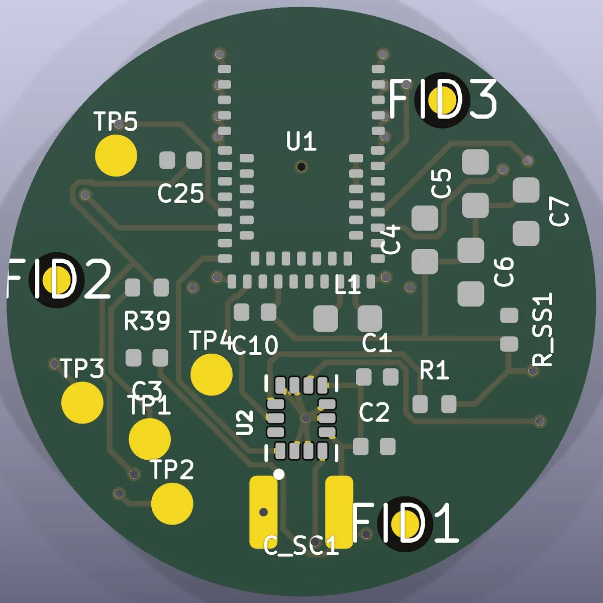
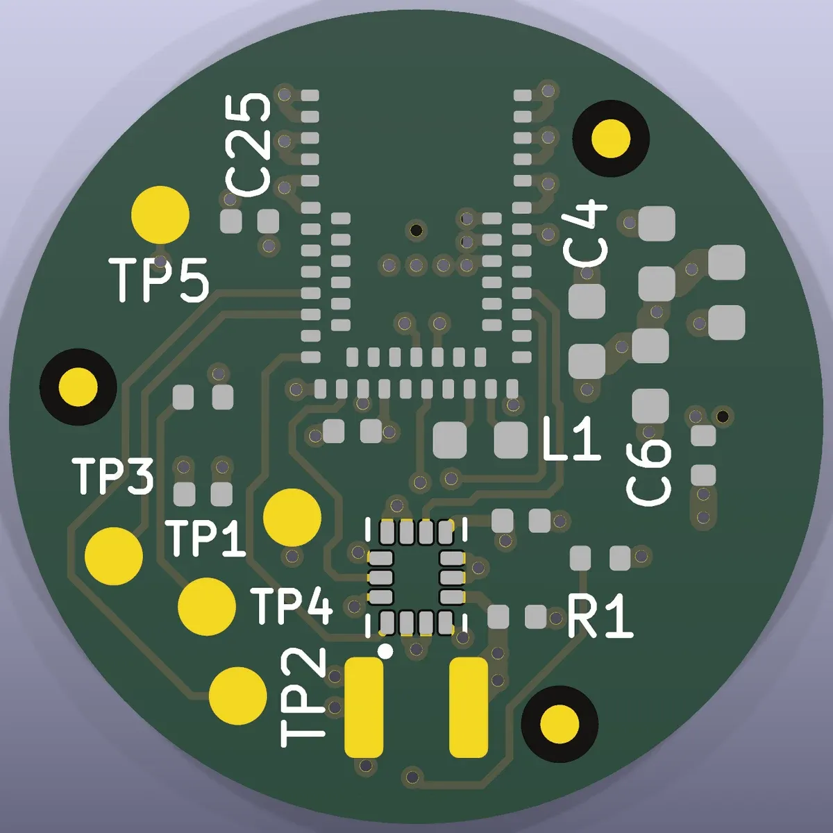
What the engineer did was not finishing the last 4%. He went back through part of the 96% I thought was done.
Layer usage was different too
The difference is hard to see from the front of the board. Comparing the inner layer used for routing makes it clearer.


Before the handoff, 6 nets used this layer across 12 trace segments. After, 3 of the original 6 dropped out and 5 new ones came in, for 8 nets total on that layer. Segments went from 12 to 79.
Across the whole PCB, vias went from 37 to 58 and trace segments from 151 to 282. At a glance it got more complicated. Yet the actual paths of the key nets above got much shorter.
So he was not minimizing via count or segment count. He spent more vias and more segments where they were needed while rebuilding the whole topology around which net belongs on which layer. The auto-router and the human were optimizing different things.
How those 11 hole clearance violations went away
The 11 DRC violations left at handoff were all hole_clearance. Only 5 vias actually caused them, and the same via colliding with several nearby copper objects added up to 11. The required hole clearance was 0.25mm and the measured values ran from about 0.2017 to 0.2423mm.
On the returned board all of them were gone. The via spec had changed at the same time. The drill stayed at Ø0.3mm but the pad grew from Ø0.5 to Ø0.6mm.
I read the relationship wrong at first. hole_clearance is the distance between the drill hole and other copper, so if the drill is unchanged, growing the pad alone cannot clear an existing violation. That part was right.
But pad size does affect whether the same violation gets created again on the next routing pass. The original via looked like this.
pad Ø0.5
drill Ø0.3

annular ring = (0.5 - 0.3) / 2 = 0.10mm
If the auto-router only guarantees 0.1mm copper-to-copper clearance, the distance from the drill edge to other copper works out like this.
0.10mm annular ring + 0.10mm copper clearance = 0.20mmThat is 0.05mm short of the 0.25mm KiCad asked for. Grow the pad to Ø0.6mm and the annular ring becomes (0.6 - 0.3) / 2 = 0.15mm. Add the 0.1mm clearance and you land on exactly 0.25mm.
So growing the via pad does mean something as a way to stop producing the same class of violation when routing new copper. But copper already sitting 0.20mm away does not move because a pad got bigger. Clearing the existing 11 required the copper in those spans to be re-placed as well.
Comparing the actual PCB files, the routing geometry at all five offending locations had changed. What the output files cannot tell me is whether the engineer deleted and redrew those spans by hand, or whether they changed during a reroute under the new via rule. That is as far as the data goes.
Our own brief was wrong too
Of the 13 DRC problems the engineer reported first, 10 started with the requirements we sent rather than the PCB. The battery pad itself sits inside a particular keep-out area, and we wrote that no copper may go in that area. We never stated that via-in-pad was an allowed exception, so read literally it was an impossible requirement. The other 3 came from his environment not having the same component and footprint files we do.
Some of what the human “found” was not a flaw in the design but a flaw in the specification and the environment. That distinction matters when you automate this too.
Turning his fixes into the next set of rules
The PCB itself was finished by the contract work. My interest moved elsewhere. What will the agent do when it meets the same problem on the next board?
So I did not simply store his revision as an answer key. I parsed the before and after PCBs and extracted the per-net differences.
- trace length
- via count
- layer used
- routing topology changes
Out of those differences I built reusable routing techniques. It started at 12 and has grown to 16 as later work turned up more. Two of them matter as examples.
- T1: via-size-normalization. Bring the via spec the auto-router uses in line with KiCad and the fab rules.
- T2: rip-up-and-reroute. Even for an already-connected net, if the topology is bad, delete the existing routing and route it again. All four nets with the large length reductions above are T2.
The problem is that the agent cannot execute T2 directly. The technique registry records which function performs each operation. Operations with no function to run yet get the value gui_card, which hands them to a human. Seven of the 16 registered techniques are in that state.
And rip-up-and-reroute, the highest-impact technique from this whole engagement, is one of the seven. Put honestly, that is the current level of automation. It could learn them, but close to half of them it still cannot execute.
There is one more principle I added. When the agent’s confidence in a judgement falls below a threshold, it does not force a routing technique. Instead of guessing and modifying the PCB, it hands off to a human. In hardware, knowing where to stop automating sometimes matters more than automating wrong.
Testing whether the learned rules get reused
The next question was this. Do the rules extracted from the contract work end as a one-time explanation, or can the agent reuse them?
To find out, I had the agent handle three problems of the same kind without being shown the engineer’s final revision. The pass conditions were fixed in advance.
| Check | Threshold | Result |
|---|---|---|
| Does a clock trace run too close between pads | edge clearance at least 0.15mm | 0.105 / 0.115mm, handed to a human |
| Are the vias around SWD/UART too dense | at least 1.0mm centre to centre | pass, 1.031mm at the closest |
| Do clock/data intrude on another via’s clearance zone | at least 0.58mm from the via centre | pass, zero violations |
By the thresholds fixed in advance, two of the three passed. Calling it 2/3 is still hard to justify.
The second one cleared the 1.0mm pre-set threshold at 1.031mm, but recomputing the geometry afterwards showed the two clearance zones need about 1.25mm to actually stay apart. It passed the test while the test itself was not strict enough.
The first one the agent did not fix; it handed it to a human. That is not a clean success either.
One thing did change from before, though. On the first auto-routing run the problem sat right there in the DRC report and I only worked out what it meant much later. This time the condition the agent could not solve surfaced explicitly as manual work. That difference was worth something.
There is a limit here too. For some of the techniques and classification rules, git history alone cannot fully reconstruct that they existed before the test. So I did not count that part as evidence of learning.
The human is still better at some of it
The engineer redrew the SWD traces without vias and reduced their inner-layer usage as well. My replay did not get to that level.
There is a more important limit. There is no control group. I never re-ran the same agent without the new routing techniques, so I cannot causally prove the improvement came from them.
And the PCB the techniques were extracted from and the PCB the replay was tested on are the same product family. So what I have confirmed is that some judgements reproduce within the same PCB family. Whether the same techniques work on a different board is still unknown. The real transfer test has to happen on the next prototype.
The automation itself was wrong several times
The PCB routing was not the only thing going wrong. At one point the routing script was not running properly at all. The commit log carries this.
route.py did not run at all — SWIG ownership trap, plus two clobber hazardsA SWIG object ownership problem kept route.py from running, and for a while I was analyzing leftovers from an earlier run as if they were current results. I was analyzing a stale artifact. The agent also asserted that “there is no more room inside Ø21mm”, a condition that turned out to be wrong when I measured the actual geometry again.
So PCB automation was not the only thing needed. I also needed instrumentation that verifies the automation actually ran, and that the basis for a judgement matches the real geometry.
These failures went into the routing techniques and the checklist too. Recording only what worked cannot stop the same failure twice.
No evidence the board works yet
Five PCBs are on order. Four-layer FR-4, 0.8mm, Ø21mm, ENIG. Nothing has arrived.
The first order also skipped an assembly review. I picked a 0.5mm pitch 14-pad LGA package while planning to assemble it myself. Independent of PCB routing, that is a part my bench cannot handle.
There is a more important fact. The boards on order predate the routing technique registry as it stands now. So this workflow has never built a new PCB end to end.
What I have confirmed so far is the routing process. Whether it boots on power-up, whether the sensor works, whether RF and power are clean, none of that is known yet. Those answers come off the bench once the boards arrive.
So where do you call a human
A few signals turned out more useful than the DRC count.
- DRC falling while unrouted nets rise. Widening clearance cleared 11 DRC violations, but unrouted nets went from 6 to 15. The number improved and the routing got worse.
- Nothing wrong in DRC, but net roles not reflected. VBAT, GND, and the SPI clock all routed on the same 0.2mm policy is the example.
- The agent not confident enough about which technique to use. In that case it does not guess and edit; it hands off to a human.
So I no longer use DRC as the final verdict. Passing DRC is necessary but not sufficient. Before fabrication I check a separate manufacturability gate alongside it.
And if you use a contractor, getting the result in a form you can diff against the previous revision is worth far more than receiving a finished PCB file. The routing techniques here came out of exactly that difference.
Seven of the 16 techniques still need a human in a GUI. The number I most want to see on the next PCB is not DRC zero. It is how far those seven come down. That is the number that shows whether this automation is actually getting better.

Comments
Loading comments...